PCB layout - JHarvey

From DIY contraptions to sophisticated FreeEMS-specific designs! Plus general hardware development!
Post Reply
User avatar
jharvey
1N4001 - Signed up
Posts: 1607
Joined: Tue Jun 10, 2008 5:17 pm

PCB layout - JHarvey

Post by jharvey »

I'm starting to think about the PCB layout parts. I've still got a ways to go before I really get into it, but have started planning now. Here's a quick sketch showing my general plan for the layout.

Image

I'm picturing the general stuff like 5V_reg, MAP, ect sitting in-between the tech art's connectors, and then two wings that go in either direction, on for injector (power inductive) drivers, and another for ignition (lower power) drivers in the other direction. That way it can grow to larger or smaller motors as time goes on. Power devices like the 5V reg, and PIP's will hang off one end, where they can be attached to a heat sink.

I'm not planing on a board connector like many ECU's have, I'm planing on individual wire lead terminations going straight to the board. The connectors will be harness type. This should help reduce the number of places you can have a bad connection, as well as allow for replacement when you have a bad connector.

That's the plan for the moment. Any thoughts?

Any one know where you can get colored PCB's? I see my PSoC cube comes in a blue that colors quite nicely when light by LED's. I'm curious what colors exist. Is clear available?
User avatar
Fred
Moderator
Posts: 15431
Joined: Tue Jan 15, 2008 2:31 pm
Location: Home sweet home!
Contact:

Re: PCB layout

Post by Fred »

If I interpret your ideas correctly you want the ignition and injection connections at opposite ends? I think that's not overly practical because of the space required to properly route wires from those ends to a single exit point.

I was in the mindset that we should have all low power low noise inputs together on one connector/harness at one end and all the noisey high power/current stuff on another at the other end. Various people gave me stick about these beliefs and I think they are right at the end of the day. Probably we want all wires entering and exiting at the same end of the case.

I'd additionally like to point out that the TA card has a DB9 on board that needs to be exposed to the world. This limits your location for it somewhat as it has to sit on a connector panel end/side for that to be accessible. You could desolder it and do your own thing there, but I don't think we should force people to desolder the connector to make a functional system.

When you say "lower power ignition drivers" do you mean the to92 buffers I spoke of? If you mean full to220 IGBTs (which could be good to support even if I don't use them on mine) then they are significantly noisier and higher power than a high Z injector driver.

I'm going to do a sketch now and post it up with a few ideas on how it could work. Back soon.

Fred.
DIYEFI.org - where Open Source means Open Source, and Free means Freedom
FreeEMS.org - the open source engine management system
FreeEMS dev diary and its comments thread and my turbo truck!
n00bs, do NOT PM or email tech questions! Use the forum!
The ever growing list of FreeEMS success stories!
User avatar
jharvey
1N4001 - Signed up
Posts: 1607
Joined: Tue Jun 10, 2008 5:17 pm

Re: PCB layout

Post by jharvey »

Good notes, Perhaps it should be one wing, with a top and bottom... That would help prevent running the power wires over the middle of the board.

I just released schematic A.05, perhaps you could comment on wire label names and the ignition driver schematic. I'm hoping to have these set's of schematics as rock solid as possible before I copy them making the multiple schematics I need to make the PCB.

This version doesn't plan for O2, or other inputs. That is that the current game plan right? I'm trying to leave room for them, but not focusing on them right now.

I tried to make it such that the general section can expand down, injectors can expand up, and the ignition can expand down.

I'm playing Jonny Electrician today, so I'll be off line until this evening, so take your time on a response.
User avatar
Fred
Moderator
Posts: 15431
Joined: Tue Jan 15, 2008 2:31 pm
Location: Home sweet home!
Contact:

Re: PCB layout

Post by Fred »

jharvey wrote:I just released schematic A.05, perhaps you could comment on wire label names and the ignition driver schematic. I'm hoping to have these set's of schematics as rock solid as possible before I copy them making the multiple schematics I need to make the PCB.
I may be able to have a look later today. I'm already copping crap for taking too long to go out (on way out soon).
This version doesn't plan for O2, or other inputs. That is that the current game plan right? I'm trying to leave room for them, but not focusing on them right now.
O2 is just a generic ADC input as you have already designed. It's non essential, BUT, it should definitely be included in the design as it is just a pig to tune without one...

TPS, CHT, IAT, O2, MAP, atmos pressure, BatV, RPM x 2

The only one we can afford to drop is the atmos pressure if we have to, though it would be nice to have that.

My rugged block design :

Image

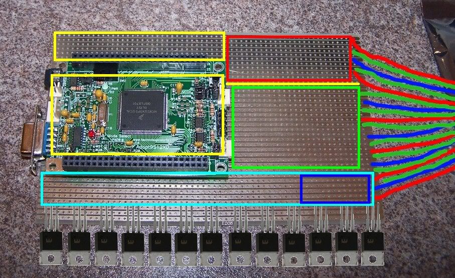
Yellow = ADC input conditioning and signal path
Red = RPM signal conditioning
Blue = power supply circuit
Pale blue = heavy traces and output conditioning stuff
Green = proto pads and also (I forgot) battery reference conditioning

Additionally I would REALLY like some 3mm LEDs paralleled with the output and RPM input circuits for a visual of proper operation, and perhaps some GPIO pins attached to LEDs on the front panel just to use as generic on car debugging in the short medium term.

The image is about 1:1 scale, but I have no idea how much room you need for everything. I do think putting power stuff close to connector/wiring is good though. I also think putting ADC stuff far away on the opposite side to the FETs/IGBTs/REGs is a good idea. Perhaps aim to put the TA board on the far side if that doesn't stuff you for routing from the second header. I think the RPM inputs should be conditioned close to the IO wiring too.

The four corners of the TA board should be supportable by screws/standoffs, so include those.

Based on my VERY rough diagram I make it 13 to220 packs. 2 regulators cuts it to 11, 1 cuts it to 12,

4 injectors or 6 injectors
1 fuel pump FET
1 regulator or 2 regulators

Leaves 3 - 6 spare FETs/IGBTs

How about :

4 Injector FETs
4 Ignition IGBTs
2 Regulators (both 5v)
1 Fuel pump FET
2 Spare FETs

That way as a stand alone unit it can run a 4 cylinder properly with 2 spare outputs and a solid power setup.

On second thoughts considering how easy it is to add more boards to a TA based setup, scratch the proto area and use that space to make the rest of the basic features more complete and robust. You might need the space anyway.

Lastly, you may not be able to get 13 to220 on there. If not, 11 is enough to do what needs to be done.

Gasp :-)

Fred.
DIYEFI.org - where Open Source means Open Source, and Free means Freedom
FreeEMS.org - the open source engine management system
FreeEMS dev diary and its comments thread and my turbo truck!
n00bs, do NOT PM or email tech questions! Use the forum!
The ever growing list of FreeEMS success stories!
User avatar
Delta
LQFP112 - Up with the play
Posts: 111
Joined: Fri Jul 25, 2008 8:04 pm
Location: Perth, WA, Australia

Re: PCB layout

Post by Delta »

I think that looks like a very reasonable layout. What are your plans for heatsinking - An alu bar and then screwed to the case, or just fets to case??
User avatar
Fred
Moderator
Posts: 15431
Joined: Tue Jan 15, 2008 2:31 pm
Location: Home sweet home!
Contact:

Re: PCB layout

Post by Fred »

OK, I mocked it up with 12 FETs on one side of a euro card and it fit's ok, but 13 would be too tight.

Image

You could potentially put to220 stuff down both sides of the board, but I strongly doubt there will be enough space to fit support circuitry for them all on the board. I guess we could populate both sides of the board with components?

Here is a car amp that has the dual side layout. I've worked on these quite a bit and they are very convenient, well protected physically, easy to access the top side of etc.

Image

I wonder if we could get bulk deals on extrusions of ally in that shape for cheap based on an existing die made for car audio use?

Although there probably isn't room for support for 24 FETs etc on one board with input stuff on there too, you could still put them down both sides, but just put six on each side at the wires end to keep them far away from the CPU and input stuff? Using both sides will double the heatsink if a bar is used and spread the heat load out at the very least. Whatever we do, the thermal mass of the bus bar used should be large enough such that each component just contributes to the overall heat (low thermal resistance along it's length) then it only has to be good enough for the average heat. The device making the most heat will be the CPU power supply regulator. The rest should run fairly cold (possible exception of IGBTs if used).

I'm going to open your pdf now and have a read/critique/think. I'll probably be most critical of that power supply circuit. I hear the guy that designed it had no idea what he was doing (that's me).

Fred.
DIYEFI.org - where Open Source means Open Source, and Free means Freedom
FreeEMS.org - the open source engine management system
FreeEMS dev diary and its comments thread and my turbo truck!
n00bs, do NOT PM or email tech questions! Use the forum!
The ever growing list of FreeEMS success stories!
User avatar
jharvey
1N4001 - Signed up
Posts: 1607
Joined: Tue Jun 10, 2008 5:17 pm

Re: PCB layout

Post by jharvey »

I'm thinking of going with SMT on most parts. I think most all parts can come in SM0805 packaging, so I'll toss that in the footprint filter for resistors and diodes, perhaps many of the caps as well.

Any recommended footprint's for any of the components?
gearhead
LQFP112 - Up with the play
Posts: 120
Joined: Sun Feb 03, 2008 9:30 pm
Location: Chicago, USA

Re: PCB layout

Post by gearhead »

First off, I am not too concerned about LEDs. I mean, if I want to see if it is working, I would connect my laptop to the ECU and see what it is doing. I think they consume board space and are unnecessary. On the bench, there is the JimStim and in the car, there is a laptop. $0.02

I was envisioning a row of to252s (dpak) along the top edge and bottom edge if necessary. to220 will work as well, but are more hassle wrt heat sinking, etc. The vnd5n07's are avail in dpak. The IPAK shows as available, though my experience that it is not readily available. I have a sleeve of 5 or 6 of these at home and have not been able to get any more. The dpak version is available through digikey. For heat sink we can clamp a bar across a group of them with screws placed every 4 devices. $0.02. large enough to be easily solder-able small enough to pack tightly and plenty of options with heavy current capability.

http://www.st.com/stonline/products/lit ... nd5n07.htm

This shows package type and characteristics of these which may be better suited to ignition duty. In my install, I will be needing BS170s for this as will Fred...
http://www.st.com/stonline/products/pro ... bt0307.pdf

For low current (to92) devices, we may consider BS170. These are not protected, but should not need to be. Just a 1k gate resistor and a 100k pull down on the gate. Seem to be readily available and easily package-able. 3V turn on voltage should be adequate.

http://www.fairchildsemi.com/pf/BS/BS17 ... escription

Gearhead
davebmw
LQFP144 - On Top Of The Game
Posts: 331
Joined: Sun Jul 13, 2008 2:58 pm
Location: South Wales, UK

Re: PCB layout

Post by davebmw »

I reckon a board about 180 mm wide and 160mm deep with 2 ally heatsink bars mounted vertically either side with TO220 IGBT, FET, and reg packages mounted vertically to save real estate.
The CPU shold be centre back away from the main connector edge and all input conditioning done near the main connector.
Forget the main proto area just provide a couple of big headers to access all the Aux IO ports. anyone with expansion plans can hardwire, veroboard or spin their own PCB's to take advantage of the extra IO's.
It should make for a clean design with easy to obtain and fit parts and quite compact too.

I will sketch something up tomorrow and post it.
93'BMW 325is M50B25TU, Rebuilt 06/06, JE10.5:1, polish&port. Scorpion BB, K&N CAI, TEJ21 WBO2, '07 M3 Evo 18" 225F, 255R, EBC Kevlar, Bilstien Sprint, Polyflex. Head rebuild Oct'08, OEM+FSE FPR, MS2v3.0_DJB Custom, Extra 2.0.1
User avatar
Fred
Moderator
Posts: 15431
Joined: Tue Jan 15, 2008 2:31 pm
Location: Home sweet home!
Contact:

Re: PCB layout

Post by Fred »

If we move away from a standard board size, what will we do for a standard case? I really like the idea of 160x180ish board with a more complete circuit topology and less crowding, but if we have to get CNC custom cases we are shooting our feet budget wise. Bang for buck is high on my agenda, I don't know about you guys, but I'm hoping for maximal performance from both hardware and firmware for minimal monetary cost.

I have to say, I don't like the idea of SMD resistors, I think standard 1/4 watt size through hole is the way to go there. You can even get high power handling ones in the same package if need be.

Me and gearhead will always disagree on the dpack vs to220 thing, but I'll just say I'm with Dave on vertical mounting of to220 parts provided we can get a case. If we are vertically mounting there is nothing to stop us putting bars across the middle of the board either like this :

Image

Image

Note : That is a real aftermarket ECU with a single layer board that runs one of our members cars! I think with 2 whole layers we should be able to do a great job of laying it all out.

Now, about those cases....

Fred.
DIYEFI.org - where Open Source means Open Source, and Free means Freedom
FreeEMS.org - the open source engine management system
FreeEMS dev diary and its comments thread and my turbo truck!
n00bs, do NOT PM or email tech questions! Use the forum!
The ever growing list of FreeEMS success stories!
Post Reply