Page 5 of 8
Re: Power Supply Design - Input Protection Scheme
Posted: Wed Dec 26, 2012 5:02 pm
by DeuceEFI
I have placed an engineering samples order with TI for some TL-431's and some LM-431's for testing purposes.

Re: Power Supply Design - Input Protection Scheme
Posted: Thu Dec 27, 2012 12:46 am
by Dan
TonyS wrote:Hi Dan,
The schematic shows the upper "REF" resistor connected to the base of the transistor. Should it be connected to +5V SWITCHED instead?
Thanks,
Huff
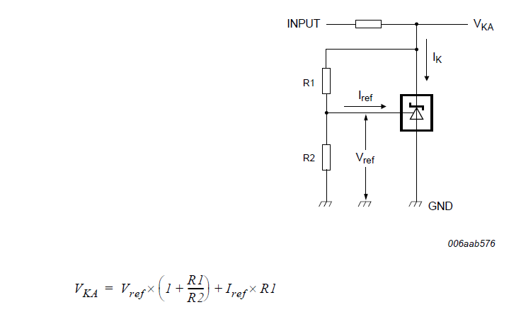
EDIT: Huff, Refer to screenshot of datasheet below. I think you may be correct (I was tired), as the datasheet example current limits the supply. Whereas we just want to current limit the TL-431. Thanks for pointing that out.
Re: Power Supply Design - Input Protection Scheme
Posted: Thu Dec 27, 2012 12:48 am
by Dan
DeuceEFI wrote:I have placed an engineering samples order with TI for some TL-431's and some LM-431's for testing purposes.
Sweet, I am ordering some today too! (they are in stock with E14 so I should have them tomorrow)
Re: Power Supply Design - Input Protection Scheme
Posted: Thu Dec 27, 2012 12:58 am
by Dan
Huff/Fred/Others,
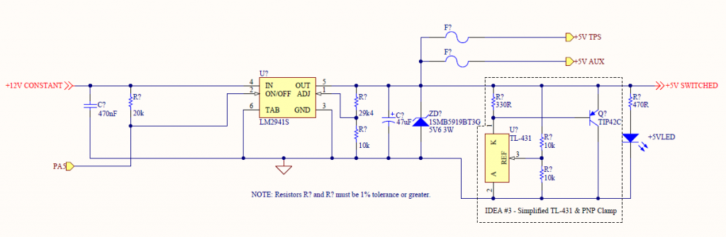
Corrected schematic for you!
Cheers,
Dan
Re: Power Supply Design - Input Protection Scheme
Posted: Thu Dec 27, 2012 4:37 am
by Dan
components ordered! shall have them in my hands tomorrow!
weekend testing madness begins!
Re: Power Supply Design - Input Protection Scheme
Posted: Fri Dec 28, 2012 2:01 am
by Dan
Bah! E14 were busy yesterday so my bits wont be here till this coming Monday. Testing will occur then
Re: Power Supply Design - Input Protection Scheme
Posted: Sat Dec 29, 2012 4:05 pm
by DaWaN
Dan wrote:Huff/Fred/Others,
Corrected schematic for you!
Cheers,
Dan
With this schematic I think the 5v6 zener can be omitted as it will never come into action
If I get this correctly the TIP42 is secured by the polyfuse ? Because the clamp will now clamp as much current as the transistor can handle, you can go easily past the thermal limitations of the transistor without fuse.
Re: Power Supply Design - Input Protection Scheme
Posted: Sat Dec 29, 2012 6:56 pm
by Fred
Yeah, I mentioned the Zener being superfluous to him too :-)
The TIP42C shouldn't ever come under any load from inside the board, and the poly fuses are what it's mainly there to do, prevent them from pulling things high. Obviously if they were omitted/bridged then the clamp would cook :-) For any other light pull up through an ADC 470 ohm, it'll be massive overkill. In general it shall sit dormant and unused except during installation ah la n00b :-)
TIP42C doesn't have to be the transistor of choice, either, just something capable of handling the trip and hold currents of one fuse. Obviously over-rated == better, though, but not to the point of blowing away board space.
Fred.
Re: Power Supply Design - Input Protection Scheme
Posted: Sun Dec 30, 2012 9:20 am
by Dan
yep the 5V6 zener is virtually obsolete if the clamp circuit works and can be configured as we require it (I copied current RavAGE schematics when I added in the "clamp circuit" above).
agreed, TIP42C probably isn't what will be used, any PNP transistor that meets what Fred has stated above should work perfectly fine!
I am testing this tomorrow (hopefully)
Re: Power Supply Design - Input Protection Scheme
Posted: Sun Dec 30, 2012 6:55 pm
by TheRevva
Noob alert... (So please correct me where I am wrong as appropriate)
I'm simply trying to follow the reasoning behind these design decisions.
The way I 'read' the schematic, it will protect the +5vSwitched from over voltage (and, as has been mentioned, the 5v6 Zener looks somewhat superfluous now).
However, it will NOT protect the +5vTPS and +5vAux lines at all.
Thus, if some IDIOT (like me) somehow connected +battery to the +5vTPS line, this line WOULD shoot up to battery (and therefore the actual TPS wiper input would jump up accordingly possibly causing the TPS analog input protection to activate.
(The TPS would still function, but it would be 'read' as full scale from about 5/12 of its wiper travel through to WOT)
I'm not 100% certain what is connected on the +5vAux line. My 'assumption' is that it's for external Hall Effect / Opto sensors.
As far as I'm aware, the majority of such sensors will quite happily survive on full battery voltage and for those that cannot, it's NOT the fault of the EMS!!!
Furthermore, I understand that most such sensors use an open collector type output and as such they would not affect the corresponding EMS input.
However, there _are_ some sensors with internal pull ups that might feed +battery back into the unit (thereby activating the OVP on the associated input)
Assuming I have correctly interpreted it all, it sure looks good to me and gets my +1!
Technically, it would be feasible to place similar OVP directly onto the +5vTPS and +5vAux lines AFTER the polyfuses in order to try to 'crowbar' them back to +5v, but that's FAR beyond the scope.
IMNSHO, the EMS unit should only be designed to protect ITSELF from idiots like me. It does not need to be designed to protect devices external to itself.
Even so, that 'protection' needs to remain 'reasonable'. I don't envisage a need to include EMP hardening (or even against hooking up my spare van de Graaf generator to random pins),