I tend to design something, work out the bugs then move on to the next part of the design that needs improvement. Normally I take notes and add those to the schematics or to the TODO list, but those 10uF caps were something that Fred and I discussed 2 years ago when I started working on the Jaguar schematics.
You are welcome.Arttu wrote:Thanks for comments.
Yeah, I tend to make the schematics as clear as possible and to include notes as to why some things are drawn the way they are or if some components are not necessary for a particular application or if they should be different values.Arttu wrote:Apparently we have slightly different point of view to using schematicsI'm using it to just define logical connections i.e. which pin connects to which net and so on. Signal routing is completely up to layout phase.
Your method may work for you, if you remember in what order the trace routing should occur. I tend to make that clear in my schematics. This makes it easier for someone else to follow what is being accomplished.
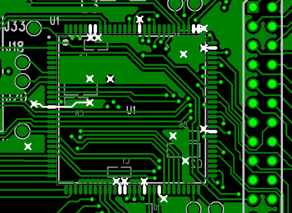
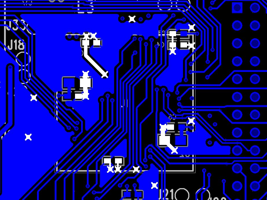
Good to know that you did that, but since the only things you have shared so far are the schematics and the component placement diagrams the people (including myself) reviewing your idea can't see that is what you did. I would recommend sharing the trace routing as well so we can see that you have the ground plane and Vcc connections correct.Arttu wrote:So even though some power supply/ground pins are connected together before the capacitors in the schematic on the board each pin pair has own decoupling cap in close proximity.
This *might* be ok, without seeing what modifications you have made to the board you are plugging this into, I can't comment one way or the other...Arttu wrote:There is a couple of 10uF bulk capacitors on the VCC net but they are located a bit further from the processor. It might be a good idea to add more of these and place them closer to the processor. For battery voltage fluctuations there is more capacitance on the main board.
Arttu wrote:I have to admit that I intentionally omitted that star shaped grounding scheme suggested on the datasheet
You may run into noise on your power supply to the MCU or even having the MCU reset when it shouldn't or at a time that could be catastrophic to your engine... This may be a good test on the bench, but I'm not sure I would put it in the engine compartment and expect it to be OK.
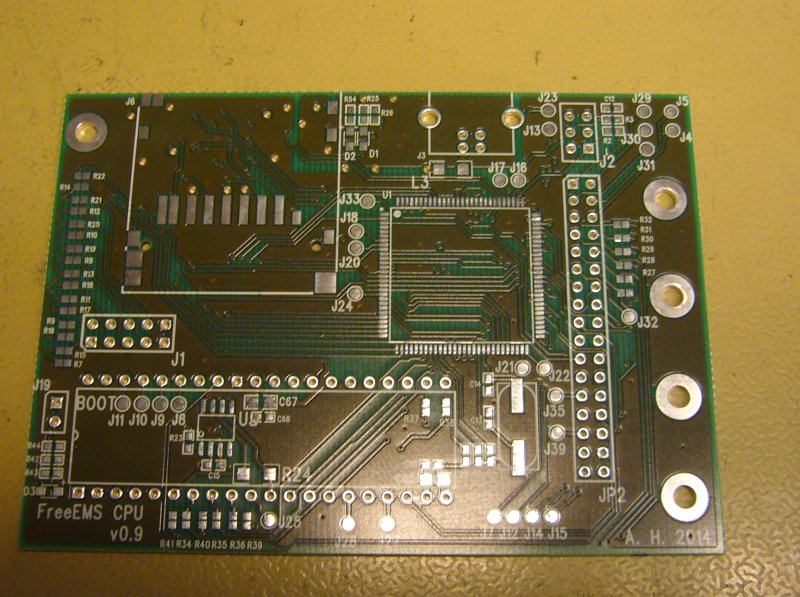
OK, keep us in the loop in the future before you place the PCB order so we can go through the design to weed out possible gotchas.Arttu wrote:At the moment the PCBs are on the way from factory to me. So let's see how they work. If they have any noticeable issues I'll fix them for the next revision.